IC substrate
.png)
| Encapsulated Type | Trandition Encap ( QFP、BGA) | Wafer Level CSP |
|---|---|---|
| Advantage |
|
|
| Disadvantage |
|
Less I/O Pin A(<100) |
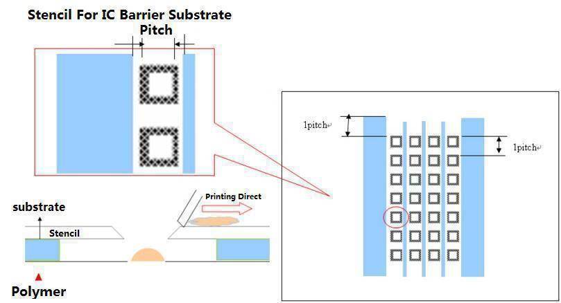
WAFER LEVEL-CSP Flux Stencil
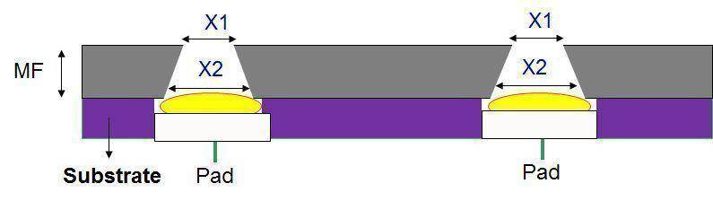
- PAD Opening Design: X1: Opening(Upper),X2=Opening(Lower) / X2 – X1 = 2~6um(Adjustable)
- Stencil Thickness (MF) : MF : 20~100um(Adjustable)
- Tension (N): 20~34N(Adjustable)
WAFER LEVRL CSP - Ball Stencil
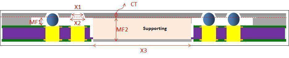
- PAD Opening Design: X1 is based on the solder ball size ; X3 – X2 = 2~6um(Adjustable)
- Stencil Thickness (CT): CT:15~30um(Adjustable)
- Metal Foil Thickness (MF1 & MF2) : MF1 : 80~130um(Adjustable) ; MF2:200~250um(Metal or Polymer)
- Tension (N): 20~34N(Adjustable)
The comparsion of inner surface roughness
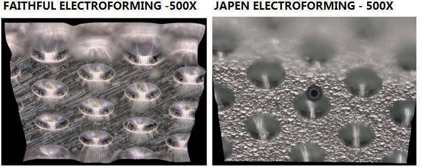
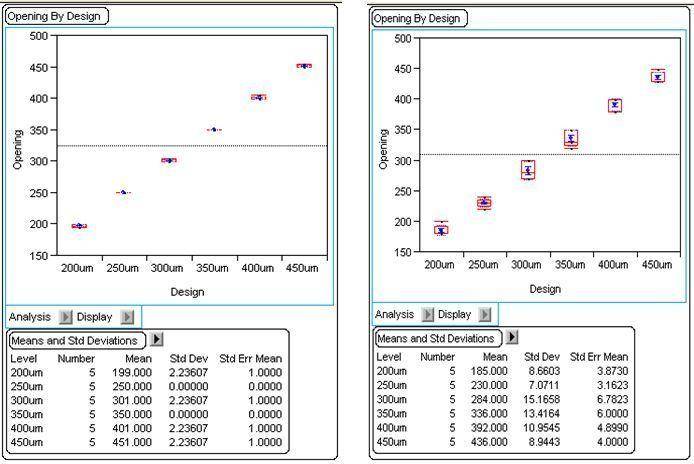
Compared FAITHFUL Stencil and Japen Stencil on Opening Dimension.
FAITHFUL's ElectroForming Stencil had better performance than Japen's Stencil.
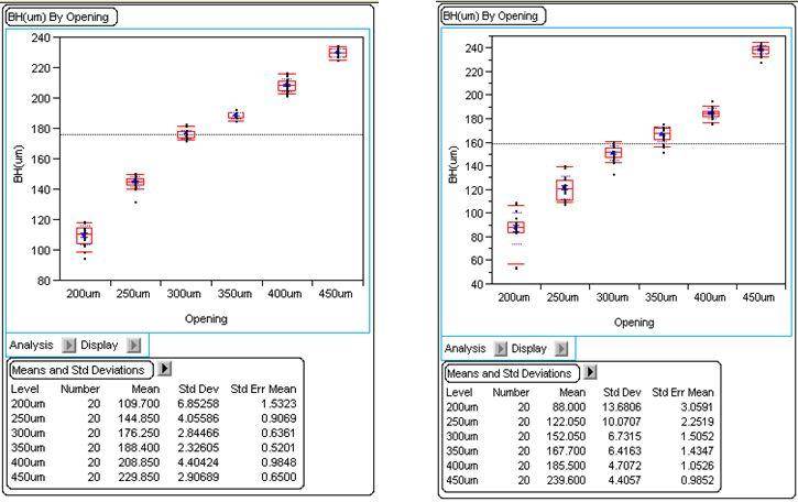
Compared FAITHFUL Stencil and Japen Stencil on Ink Deposite Performance.
FAITHFUL's ElectroForming Stencil had better performance than Japen's Stencil.
Stencil Application and Surface Technology
The Stencil Specification of Wafer Level CSP Application
| Basement Layer | |
|---|---|
| Available Wafer Size | 6~12 inch Wafer |
| Material | NiCo Alloy |
| Accumulated Accuracy: | +/-0.01%Length |
| Thickness Range(μm) | 20~200 |
| Thickness Accuracy(μm) (Pattern Area) |
20~50μm(+/-3μm)
51~100μm(+/-10μm)
101~200μm(+/-20μm)
|
| Minimum Opening (μm) | 50μm |
| Minimum Space (μm) | 50μm |
| Opening Aperture Accuracy(μm) |
+/-3μm(Thickness Range:20~50μm)
+/-5μm(Thickness Range:51~100μm)
+/-5μm(Thickness Range:101~200μm)
|
| Aspect Ratio | ≦1:1.2 |
| Support Layer | |
|---|---|
| Material | Polymer or NiCo Alloy |
| Alignemnet Space(μm) | 30μm/side |
| Thickness Accuracy(Pattern Area) |
Polymer:+/-3μm
NiCo Alloy:+/-10μm
|
| Minimum Support Area(μm) | 40μm×40μm |
| Minimum Support Width(μm) | 40μm×40μm |
| Product | |
|---|---|
| Aspect Ratio | ≦1:1.2 |
| Tension(N) | 20~34 |
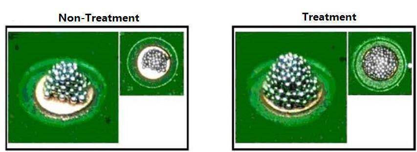
The Advantage of FAITHFUL Electroforming Stencil with polymer supporting layer
- High Accumulated Accuracy and Precised Metal Thickness.
- Using polymer supporting layer can make sure excellent stecncil flatness and the uniformity of thickness can below 3μm.
- The charateristic of Faithful electroforming stencil is long life time because we selected the Ni/Co alloy as our soultion basement.
- It can be avoid the wafer damaged issue happen by the stencil we desinged with the supporting layer on the stencil.
Diagram Index
- The space of polymer is X :50~500μm(Depend on the product design)
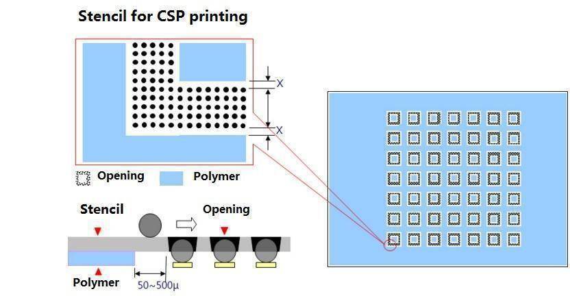
Diagram Index
- The space of polymer is X :50~500μm(Depend on the product design)